The previous article in our series on switched-mode power supplies (SMPS) covered asymmetrical isolated converter topologies. Now we will investigate several symmetrical isolated converters along with their advantages and disadvantages for different applications.
Symmetrical converters require an even number of switches. The full available flux swing in both quadrants of the B-H loop is used, thus utilizing the core much more effectively. Therefore it can produce more power than asymmetrical converters. Push-pull, half-bridge, a full-bridge converters are all symmetrical converters.
Push-pull Converter
A push–pull converter is a bidirectional converter that uses a transformer to provide galvanic isolation for the load and to provide voltage conversion (AC-DC and DC-DC).

Push-pull converters are used when there is a wide variation in the input and when the output voltage is lesser than the input voltage. They can be used at power levels in the range of 100 W to 500 W.
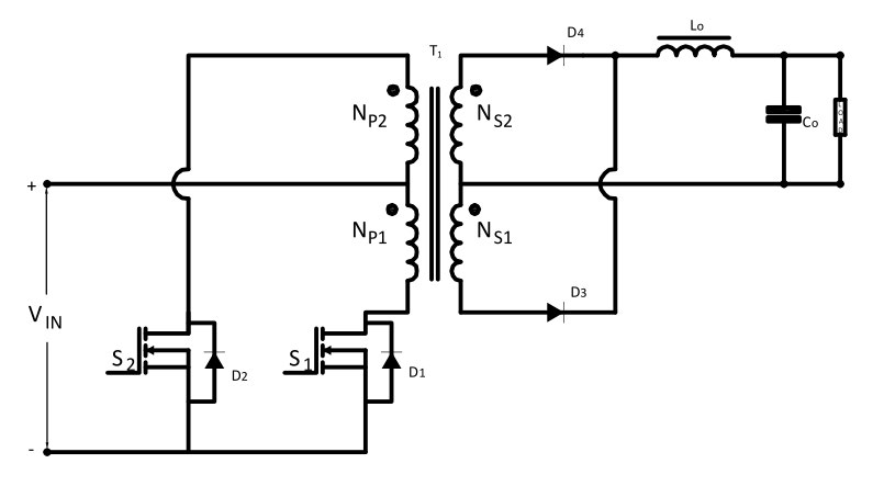
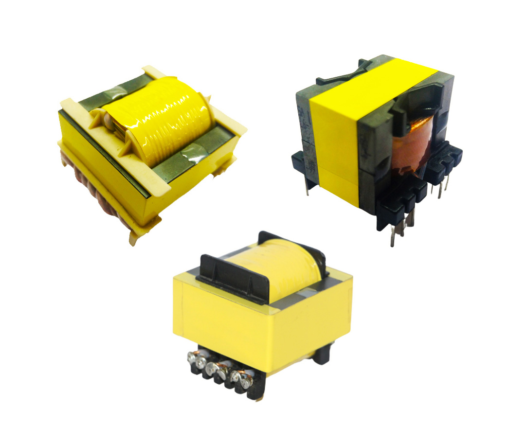
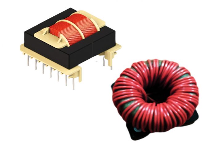
The transformer used in a push-pull converter consists of a center-tapped primary and a center-tapped secondary. The switches S1 a S2 are driven by the control circuit, with each switch driven alternately, thus driving the transformer in both directions. The push-pull transformer is typically half the size of that for the single ended types, resulting in a more compact design.
This push-pull action produces natural core resetting during each half cycle, thus no clamp winding is required. Power is transferred to the buck type output circuit during each switch conduction period. The duty ratio of each switch is usually less than 0.45. This provides enough dead time to prevent switch cross conduction. The power can now be transferred to the output for up to 90% of the switching period, allowing greater throughput power than with single-ended types.
When switch S1 is ON and switch S2 is OFF, the energy is transferred to the load through transformer secondary NS2, D4 a Lo.
When switch S2 is ON and switch S1 is OFF, the energy is transferred to the load through transformer secondary NS1, D3 a Lo.
When both switches S1 a S2 are OFF, the body diode of the switch provides the path for the leakage energy stored in the transformer primary. The output rectifier diode D3 becomes forward-biased and carries half of the inductor current through the transformer secondary NS1, and half of the inductor current is carried by the diode D4 through the transformer secondary NS2. This results in equal and opposite voltages applied to the transformer secondaries, (both NS1 a NS2 have an equal number of turns) therefore, the net voltage applied across the secondary during the Toff period is zero.
Vout/Vin Relationship

Vin > Vout
Range of duty cycle < 1
Advantages
- Power range up to several KW achievable
- To drive switches push-pull does not necessitate an isolated power supply
- Simple circuit
- High Efficiency
- Small output inductor required
- Multiple outputs possible
Disadvantages
- Each switch must block twice the input voltage due to the doubling effect of the centre-tapped primary, even though two switches are used.
- The centre-tap arrangement also means that extra copper is needed for the primary, and very good coupling between the two halves is necessary to minimize possible leakage spikes. A center-tapped primary would normally be bifilar wound, but this will cause a large AC voltage between the adjacent turns.
- The high voltage (2 • Vin) stress on the switch and 50% utilization of the transformer primary makes using the push-pull topology undesirable when the input voltage is European, Asian, the universal range (90 VAC-230 VAC), or when PFC is used. This is why push-pull topology is most favorable for low-voltage applications such as US regulation 110 VAC input direct off-line SMPS. It has also been widely used in converters operating in 12 V & 24 V battery-powered systems.
- Another problem that can occur in a push-pull converter is the magnetic flux displacement (flux walking). If the flux swing in each half cycle is not exactly symmetrical, the volt-sec will not balance, and this will result in transformer saturation, particularly for high input voltages. This magnetic imbalance can be caused by an unequal Ton period for both switches, an unequal number of turns of the primary NP1 a NP2 and the secondary NS1 a NS2, and an unequal forward voltage drop of the output diodes D3 a D4. This imbalance can be reduced by careful selection of the gate pulse drive circuitry, using a switching device, and adding an air gap to the transformer core.
- Higher component count, particularly with multiple regulated outputs.
Applications
- RF Amplifier (CAR Audio)
- AC motor drivers
- DC motor drivers
- Inverters
Half-Bridge Converter
The half-bridge converter is most popular for higher power applications (up to 500 W). It is a derivative of the buck converter that uses transformer to provide galvanic isolation for the load and to provide voltage conversion (AC-DC and DC-DC).

This topology also uses two major magnetic components, a transformer and an output inductor, but in this case the transformer core is better utilized than in a forward converter. The switching elements operate independently, with a dead time in between, switching the transformer primary both positive and negative with respect to the center point.
Dead times td between two consecutive switch conductions are absolutely mandatory to avoid a bridge-leg short circuit.
When switch S1 is ON and switch S2 is OFF, the energy is transferred to the load through transformer secondary NS2, D2 a Lo.
When switch S2 is ON and switch S1 is OFF, the energy is transferred to the load through transformer secondary NS1, D1 a Lo.
Vout/Vin Relationship

Vin > Vout
Range of duty cycle < 1
Advantages
- Voltage stress on the switch is Vin and this makes it much more suited to 250 VAC and PFC applications.
- Flux-walking problem is eliminated as the primary is only a single winding. A small DC blocking capacitor is placed in series with the transformer primary, to block the DC flux in the transformer core.
- High efficiency, high power density and the simplified transformer construction makes it ideal for medium power applications.
- Excellent transformer utilization, very low output ripple and small output inductor required.
Disadvantages
- High ripple current in C1 a C2, which have to be carefully selected so that they do not overheat.
- Isolated driver is needed for top switch which adds component cost.
- Functioning at half of the input voltage (Vin) so collector current is double compared to Push-pull scheme.
- Not suitable for current mode control.
Applications
- Well suited for high input voltage applications up to 440 V mains.
- Large computer supplies.
- Lab equipment supplies.
Full Bridge Converter
The full-bridge converter is a higher power version of the half-bridge and provides the highest output power level (up to 1000 W) of any of the converters discussed above.

Full-bridge converters use a transformer to step down the pulsating primary voltage, as well as to provide isolation between the input voltage source and the output voltage Vout.
The full-bridge converter uses four switches that operate in an alternating fashion. Two diagonal switches turn ON a OFF in one PWM cycle and then the other two diagonal switches in the next PWM cycle. The flux is reset when the other switch pair is turned ON, so duty cycles from 0 to 1 are possible. There are two power pulses transferred each cycle, enabling the use of a smaller inductor and output capacitor.
When switch S1, S4 are ON and switch S2, S3 are OFF, the energy is transferred to the load through transformer secondary NS2, D2a Lo.
When switch S2, S3 are ON and switch S1, S4 are OFF, the energy is transferred to the load through transformer secondary NS1, D1a Lo.
Vout/Vin relationship

Vin > Vout
Range of duty cycle < 1
Flux imbalance may be an issue with the full-bridge converter. An optional capacitor CB may be added so if one switch pair conducts more current than the other pair, the voltage on CB will shift up or down in a manner to equalize the current flow through the switches. The totem pole arrangement of the switches (where one is stacked above the other) is susceptible to current shoot-through from the Vbus supply rail to the return when one switch is turning OFF while the other is turning ON. To prevent shoot-through, a dead time must be inserted between each switch transition.
Advantages
- Requiring one mains smoothing capacitor compared to two for the half-bridge saves space.
- Handles of a wide range of input and output voltage levels
- High power density
- Voltage stress on the switch is Vin
- High core utilization is (full flux swing in quadrants 1 and 3) allow the use of a smaller core.
Disadvantages
- Switching devices can be expensive, so it makes sense to include proper control circuits that offer good device protection, soft-start capability, and fast, high-current driver circuits.
- The timing circuit is more complex and two high-side drivers are needed.
- Higher component count particularly with multiple regulated outputs.
- Expensive as compared to other converters since it uses more components.
Applications
- Computer mainframe supplies.
- Large lab equipment supplies.
- Telecommunication systems.
- DC servo motor drives.
- Generating AC voltage for AC motor drives.
- RF heating.
- Battery chargers.
The next article in our SMPS series will focus on resonant converters and their main applications.


