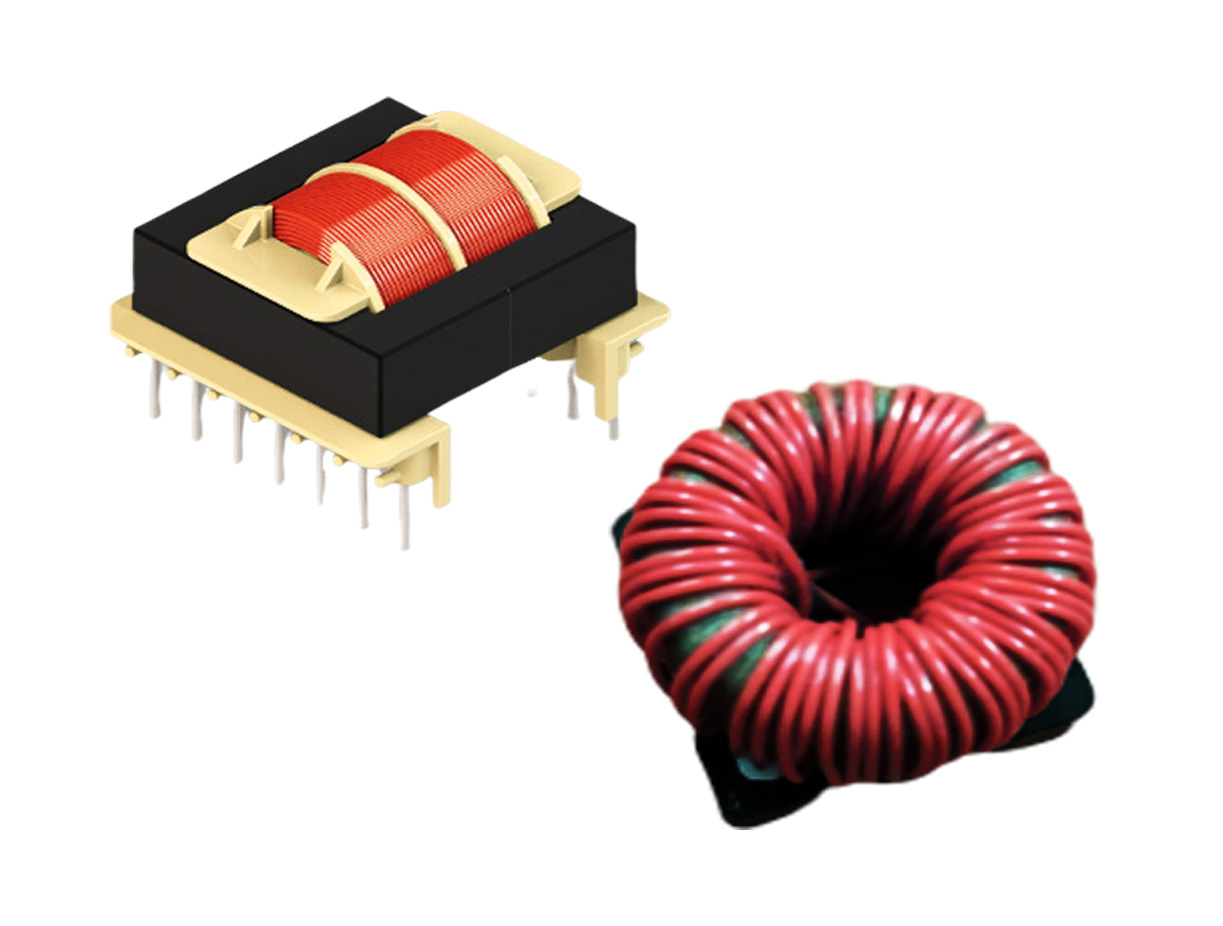
A gate drive transformer is optimized for transmitting rectangular electrical pulses with fast rise and fall times to activate or deactivate a switching device.
Despite various floating channel MOSFET/IGBT driver ICs being available, a transformer-coupled gate drive is still the better option to use for high power applications for many reasons. For example, due to the multiple numbers of galvanically isolated output windings, a single transformer can drive all switches in the bridge and also makes it easier to drive parallel switches (MOSFETs/IGBTs). It also has negative gate bias when the device is OFF which reduces dv/dt susceptibility (an excessive dv/dt rate might cause false switching or permanent damage of a switching device). Furthermore, a properly designed transformer-coupled solution has negligible delays and can operate across higher potential differences.
Gate Drive Transformers
A gate drive transformer is a transformer that is optimized for transmitting rectangular electrical pulses with fast rise and fall times to activate or deactivate a switching device. It handles low power but high peak currents to drive the gate of a power switch. Power ratings range from µW to several KW.
The gate drive transformer provides both the floating supply as well as the level shifting of the switching signal to the power semiconductor, thereby eliminating a separate floating power supply. It can be used to directly drive the power switch (MOSFET/IGBT) gates or it can be used to just isolate the control signal which is then applied to a gate driver IC. In addition, it also provides impedance matching.
When operating at high switching frequencies (> 100 KHz), designing and constructing high isolation gate drive transformers requires careful consideration in order to avoid the adverse effects of parasitic components (leakage inductance & distributed capacitance)
A gate drive transformer can also be called a pulse transformer, trigger transformer, wide band transformer, or signal transformer. The distinction is based mostly on the actual purpose of the transformer: where the transformer is used to directly drive a power device gate it is referred to as a gate drive transformer; if used only as a means of transmitting rectangular voltage signals/pulses to a semiconductor gate then it is referred as a pulse transformer. However, in general, a pulse transformer transfers a pulse of current/voltage from the primary/generating side of the circuit to the secondary/load side of the circuit with its shape and other properties maintained. If the transformer pulse initiates some action or event it could be called a trigger transformer.
Transformers have at least two windings (primary and secondary) which facilitate isolation, an important attribute. The turns ratio between primary and secondary also allows voltage scaling, but it is usually not required.
Basic Circuit
The basic circuit of a transformer-based isolated gate drive is relatively large. In addition to the transformer, it also consists of the associated reset components, such as the blocking capacitor C, primary resistor R, gate resistor Rg, back to back Zener diodes, etc.
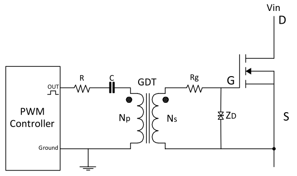
When a square pulse is applied at the primary terminals, it will be transmitted at its secondary as a square wave or the transmitted signal will be derivative of the input voltage.
The blocking capacitor C is placed in series with the primary winding of the transformer to provide the reset voltage (negative bias) for the magnetizing inductance. Without the capacitor, there would be a duty-ratio-dependent DC voltage across the winding (DC offset or “flux walking”) and the transformer would saturate. This is a very simple circuit; the amplitude of its output voltage reduces with the duty ratio increase, hence this circuit is limiting the duty cycle to less than 50%. This approach works well in switch mode power supply (SMPS) circuits, where the frequency is high and the duty cycle ratio is small.
Coupling capacitor voltage:

The actual gate drive voltage, Vc, changes with duty ratio. In addition, sudden changes in duty ratio will excite the L-C resonant tank which is formed by Lm & C. This L-C resonance can be damped by a low-value resistor (R).
The gate is driven between -Vc and VDRV-Vc levels instead of the original output voltage levels of the driver, 0 V and VDRV
Back-to-back Zener diodes are used to clamp the device gate voltage, thereby avoiding overvoltages generated by the uncoupled transformer T leakage inductance. A gate resistor Rg is used to avoid the gate transient surge current.
Core saturation limits the applied volt-time product across the windings. The transformer design must anticipate the maximum volt-time product under all operating conditions, which must include worst case transients with maximum duty ratio and maximum input voltage at the same time.
Maximum volt time product:


T = Switching period
F = Operating frequency
VPEAK = Peak drive voltage
D = Duty Cycle
The gate drive transformer is driven by a variable pulse width as a function of the PWM duty ratio and either constant or variable amplitude depending on the circuit configuration.
There are two types of transformer-coupled gate drive circuits: single-ended und double-ended.
In both single & double ended circuits, the gate drive transformers are operated in both the first and third quadrant of the B-H plane.
Single-Ended Transformer-Coupled Gate Drives
Single-ended gate drive circuits are used with a single output PWM controller to drive a high side switch and the gate drive transformer is driven by a variable pulse width and variable amplitude.
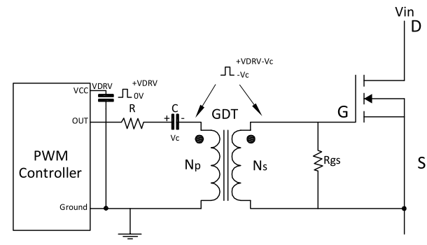
This circuit is limited to 50% duty ratio. For wide duty cycle applications such as buck converters, it doesn’t provide adequate gate drive voltage and thus a DC restoration circuit has to be added on the secondary side of the transformer (capacitor and diode). Coupling capacitor voltage increases with duty ratio increase and also reduces actual gate drive voltage (for turn on) and increases negative bias (during off time). Adding a capacitor and diode in the circuit helps restore the original gate drive amplitude on the secondary side of the transformer.
Double-Ended Transformer-Coupled Gate Drives
Double-ended gate drive circuits are used with a double output PWM controller to drive 2 or 4 switches in high power applications such as in half-bridge & full-bridge converters and the gate drive transformer is driven by a variable pulse width and constant amplitude.
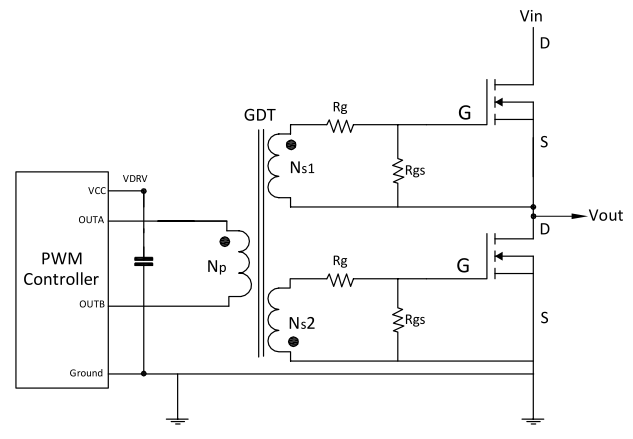
OUTA and OUTB are opposite polarity and symmetrical, when OUTA is on, positive voltage applied, When OUTB is on, an opposite polarity voltage is applied across the primary winding of the gate drive transformer. Averaging the voltage across the primary for any two consecutive switching period results in zero volts. Thus AC coupling is not needed (coupling capacitor & damping resistor are not needed in the primary side of the circuit).
Conclusion
Transformer-coupled gate drive circuits offer many advantages, especially in high-power applications. Next, we will take a closer look at the desired pulse response characteristics of a gate drive transformer, and the paramaters that influence them.

