Phase-shifted full-bridge (PSFB) converters are used to step down high DC voltages and to provide isolation in medium to high power applications (> 1000 W).

PSFB converters are similar to conventional full-bridge DC-DC converters, but with a phase shifting control. The phase shift full-bridge converter can achieve soft switching by phase-shifting the gate signals between the leading leg and the lagging leg switches without additional circuits. Therefore, the switching loss can be reduced and the efficiency can be increased.
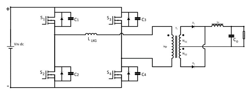
A PSFB converter consists of four power electronic switches (such as MOSFETs or IGBTs) that form a full bridge on the primary side of the isolation transformer and diode rectifiers or MOSFET switches for synchronous rectification (SR) on the secondary side. The parasitic capacitances (C1, C2, C3, C4) are connected across the switches and the inductor connected in series with the primary winding of the transformer emphasizes the leakage inductance of the high-frequency transformer.
The leg with pair switches S1 y S2 are turned on complimentarily with a 50% duty cycle with short dead time. The same is true for the second leg with pair switches S3 y S4. The control signal to switch S3 y S4 is phase-shifted with respect to the gating signal to switch S1 y S2 to allow zero-voltage switching (ZVS) transition and also to ensure that the transformer primary is either connected to the input or shorted.
When the diagonal switches are ON, Power is transferred to the load through the transformer secondary.
If either the top or bottom switches of both legs are ON simultaneously, no power is transferred to the secondary, since zero voltage is applied across the primary.
When the appropriate diagonal switches are turned OFF, primary current flows through the output capacitor of the respective MOSFETs causing switch drain voltage to move toward to the opposite input voltage rail. This causes zero voltage across the MOSFET, thus creating ZVS when it turns ON. This is possible when enough circulating current is provided by the inductive storage energy to charge and discharge the output capacitor of the respective MOSFETs.
The parasitic output capacitor of the MOSFETs and the leakage inductance of the switching transformer are used as a resonant tank circuit to achieve zero voltage across the MOSFET at the turn-on transition.
During the transition intervals, the energy stored in the resonant inductor is used to charge and discharge the parasitic capacitances of the MOSFET to achieve ZVS at turn-on.
The leakage inductance of the transformer does not necessarily need to be minimized as a larger resonant inductance allows ZVS over a greater load range. Additional leakage inductance can even be added to the transformer in order to increase the size of the resonant inductance.
Vout/Vin relationship

VIN > VOUT
Range of duty cycle < 1
Advantages
- High efficiency: 90% to 95% at high frequencies
- Voltage stress on the switch limited to Vin
- ZVS and low EMI
- Doesn’t require additional snubber circuits to reduce losses.
- Twice the power compared to a half-bridge design, excellent choice for EU line voltage (PFC pre-regulator) with output power > 1 kW
Disadvantages
- Dual high side primary gate drive
- Circuit complexity
- High circulating primary current for ZVS
- Loss of ZVS at light load current
Applications
- Industrial battery chargers
- CAR on-board chargers
- Renewable energy systems
- Telecom rectifiers
- Server power supplies
In our final article on SMPS, we will look at several design considerations to keep in mind when designing SMPS transformers.


