Our previous article on switched-mode power supplies covered the basics of power conversion and outlined the key differences between switched-mode and linear power supplies. We also established that there are two main categories of SMPS topologies: non-isolated converters and isolated converters.
In this article, we will take a closer look at non-isolated converter topologies.
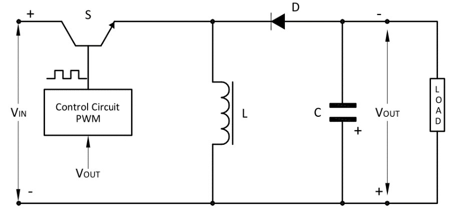
Buck Converter (Step-down)
As the name suggests, the step-down or buck converter converts a higher input voltage into a stabilized lower output voltage. It is non-isolating and ideally suited to step down voltages as a DC to DC converter. This is a relatively simple circuit with the inductor current controlled by a top switch and diode.
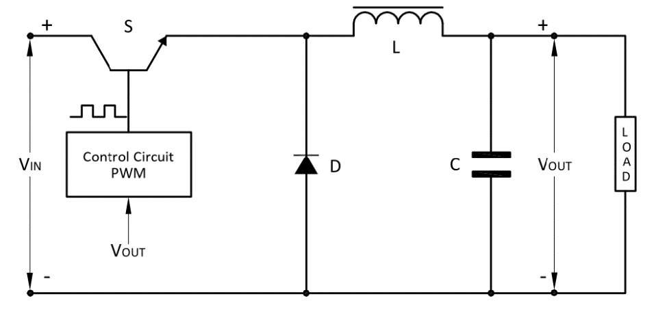
When the switch is ON, the energy is transferred to the load as well as inductor L.
When the switch is OFF, inductor voltage reverses and freewheeling diode becomes forward biased, the energy stored in inductor L supplies the load through D and L.
The LC arrangement provides very effective filtering of the inductor current. Hence, the buck and its derivatives all have very low output ripple characteristics. The buck is normally always operated in continuous mode (inductor current never falls to zero) where peak currents are lower, and the smoothing capacitor requirements are smaller.
The output voltage is dependent on the ON and OFF time i.e. the duty cycle of the square wave pulse and the expression for output voltage is as follows:

D is the top switch duty cycle, defined as the conduction time divided by one switching period
Advantages
- Buck converter is very simple and it requires only one power switch
- Efficiency of Buck regulator is about 90%
- The cost and size are low
- Line voltage variation has large tolerance
Disadvantages
- PWM regulator feedback circuit requires a minimum output ripple to regulate properly
Applications
- Battery operated portable equipments like RAM, CPU, USB etc.
Boost Converter (Step-Up)
As the name suggests, the step-up or boost converter converts a lower input voltage into a stabilized higher output voltage.
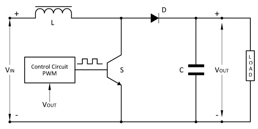
When the switch is ON, diode D reverse biased and the energy is stored in L and capacitor C supplies current to the load.
When the switch is OFF, the energy stored in L is transferred to the load through L and D.
Output voltage can be higher than the input due to the summation of the voltage pre-stored in L and VIN.
The current supplied to the output smoothing capacitor from the converter is the diode current, which will always be discontinuous. This means that the output capacitor must be large, with a low equivalent series resistance (e.s.r) to produce a relatively acceptable output ripple. This is in contrast to the buck output capacitor requirements.
The boost input current is the continuous inductor current, and this provides low input ripple characteristics. This feature makes the boost converter is an ideal choice for power factor correction application, which means Boost converter as a pre-regulator, placed before the main converter. The main functions being to regulate the input supply, and to greatly improve the line power factor. This requirement has become very important in recent years, to improve the power factor of the mains supply.
The output only depends upon the input and duty cycle:

Advantages
- This converter is able to step up the voltage at lowest component count possible.
- The input current is continuous which is very desirable for sources like Photovoltaic or battery.
- The switch used here has the common ground with the source which makes the drive circuit and control circuit arrangement easier.
Disadvantages
- The charging current of the output capacitor is discontinuous resulting in larger capacitor size and EMI issues.
Applications
- Power factor correction circuits
- Electric cars
- Battery power systems
Buck-Boost Converter (Step Down / Step-Up)
The Buck-Boost switching regulator is a combination of the buck converter and the boost converter that produces an inverted (negative) output voltage which can be greater or less than the input voltage based on the duty cycle. The buck-boost converter is a variation of the boost converter circuit in which the inverting converter only delivers the energy stored by the inductor L, into the load. Both input and output currents are pulsating, low ripple levels are very difficult to achieve using the buck-boost. Very large output filter capacitors are needed, typically up to 8 times that of a buck regulator.
When the switch is ON, the diode is reverse biased and the energy is stored in L and the capacitor C supplies current to the load.
When the switch is OFF, the energy stored in L is transferred to the load through L and forward biased diode D.
The expression for output voltage is:

Advantages
- Input voltage can be higher or lower than the regulated output voltage
Disadvantages
- Inverted output voltage
- Switch does not have a ground connection, this means that a level translator is needed in the PWM output circuit which can add cost and complexity to the design.
Applications
- Stabilizing photovoltaic cell outputs
Comparison
| Buck | Boost | Buck-Boost | |
| Output Voltage |  |  |  |
| Power (W) | 0–1000 | 0–150 | 0–150 |
| Range of Duty Cycle | 0 to 1 | 0 to < 0.8 | 0 to < 0.8 |
| Energy Storage | Single Inductor | Single Inductor | Single Inductor |
| Features | Continuous current at output | Continuous current at input | No continuous current at input and output |
In our next article, we will take a look at asymmetrical isolated converter topologies and their applications.